Basic principle of epitaxial growth On a substrate substrate (mainly sapphire and SiC, Si) heated to a suitable temperature, a gaseous substance, InGaAlP, is controlled to be transported to the surface of the substrate to grow a specific single crystal film. At present, the LED epitaxial wafer growth technology mainly adopts an organometallic chemical vapor deposition method. Introduction to MOCVD Metal-Organic Chemical Vapor Deposition (MOCVD), a new technology for preparing compound semiconductor single-film films proposed by Rockwell Corporation in 1968. This equipment integrates precision machinery, semiconductor materials, vacuum electronics, fluid mechanics, optics, chemistry, and computer multidisciplinary. It is a state-of-the-art optoelectronic special equipment with high degree of automation, high price, and high technology integration. It is mainly used for GaN ( The epitaxial growth of GaN-based semiconductor materials and the fabrication of blue, green or ultraviolet light-emitting diode chips are among the most promising specialized devices in the optoelectronics industry. LED chip manufacturing process Epitaxial wafer→cleaning→plating transparent electrode layer→transparent electrode pattern lithography→corrosion→debonding→platform pattern lithography→dry etching→degraction→annealing→SiO2 deposition→window pattern lithography→SiO2 corrosion→degglomerate→ N-pole pattern lithography → pre-cleaning → coating → stripping → annealing → P-pole pattern lithography → coating → stripping → grinding → cutting → chip → finished product testing. In fact, the production process of the epitaxial wafer is very complicated. After the epitaxial wafer is finished, the next step is to make the electrode (P pole, N pole) of the LED epitaxial wafer, and then start cutting the LED epitaxial wafer with a laser machine (previously cutting LED epitaxial wafers are mainly made of diamond knives. After being fabricated into chips, nine points are taken at different positions on the wafer for parameter testing, as shown in the figure: 1. Test the voltage, wavelength and brightness mainly. The wafer that meets the normal shipping standard parameters will continue to do the next step. If the nine-point test does not meet the relevant requirements, the wafer is placed on one side. deal with. (Editor: Wen Jing) Powerful LED Diving Flashlight Led Flashlight,Diving Flashlight,Led Flashlight Thefirst International Lighting Co., Ltd. , http://www.gddivinglight.com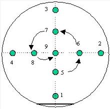
2. After the wafer is cut into chips, 100% of the visual inspection (VI/VC) is performed by the operator using a microscope magnified 30 times.
3. The chip is then fully automated, selected, tested, and classified using a fully automated sorter based on different voltage, wavelength, and brightness prediction parameters.
4. Finally, the LED chip is inspected (VC) and labeled. The chip area should be at the center of the blue film. There are up to 5,000 chips on the blue film, but the number of chips on each blue film must be no less than 1000. The chip type, batch number, quantity and photoelectric measurement statistics are recorded on the label. Attached to the back of the glossy paper. The chip on the blue film will be the same as the first visual inspection standard, ensuring that the chips are neatly arranged and of good quality. This makes LED chips (currently known as square chips on the market).