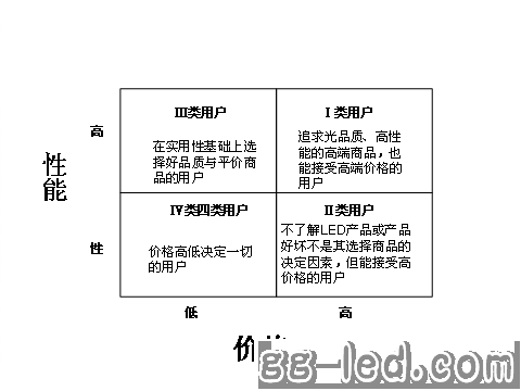
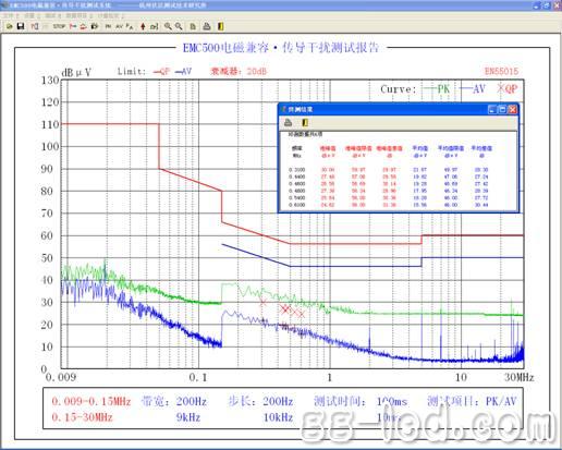
Figure 2 New LED bulbs produced by Ningbo Meiya bare crystal light engine Figure 2 LED packaging companies can divide downstream users into four categories Figure 3: bare crystal light engine conduction test Figure 4 10W bare crystal light engine test report (without cover) Figure 5 ceramic PCB substrate Figure 6 Specially designed COB light source Figure 7 Block diagram of the high voltage linear constant current driver chip Figure 8 Die IC wiring diagram Plate non-damaged desulfator with Smart pulse, Simple and Safe, Restore your battery when charging.
Product features:
EV Battery Charging Restorer EV Battery Charging Restorer,Electric Motorcycle Battery Restorer,EBike Power Battery Repair,Electric Cycle Battery Repair Shenzhen Daceen Technology Co., Ltd. , https://www.daceen-sz.com
This product design technology can bring an innovative idea to the LED packaging industry, and expand the traditional LED packaging industry up and down. In the current LED packaging industry, the marginal cost increase and the marginal revenue decline are in the current situation, and the cost profit has reached the critical point. Under the situation that the return on investment is not as good as expected, a new photoelectric engine can be obtained without further investment to increase the added value of the product. In line with the trend of integration of semiconductor products and the trend of large-scale production. The bare crystal light engine is designed to produce a new generation of LED bulbs, downlights, etc. It is very convenient and fast. Figure 1 shows the new LED bulbs produced by Ningbo Meiya bare crystal light engine. 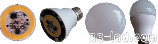
Regulations;
Electricity: input AC180-240V/100-130V/50-60HZ, power 5-12W, PF≥0.95,
THD<15%, power efficiency ≥90%, EMC meets CE and RCM certification requirements;
Heat: The thermal conductivity of the substrate is ≥25 W/m. K;
Environmental protection: in line with ROSH standards;
Use: The power AC input lead is directly soldered to the L/N pad on the module to illuminate.
The conduction test of Ningbo Meiya Optoelectronics' bare crystal light engine is shown in Figure 3. The performance meets the needs of large-scale production of LED light sources and lamps. The 10W bare crystal light engine test report (without cover) is shown in Figure 4. 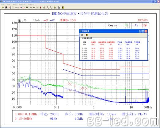
(A) a ceramic PCB, a ceramic PCB substrate <br> <br> substrate shown in FIG. 5, the ceramic substrate is an aluminum substrate has many advantages that are not. The main advantages of ceramic substrates:
1. Compared with the traditional aluminum substrate, the reflectivity of the ceramic substrate is higher, which helps to improve the light efficiency.
2. Ceramics have high reliability characteristics such as oxidation resistance, acid and alkali resistance, wear resistance and aging resistance.
3. Ceramics are insulators, which help LED lighting products pass various high-voltage tests and safety tests.
4. The thermal expansion and contraction coefficient of ceramics is small. Under high temperature environment, the surface is also relatively flat, which helps to maintain the thermal resistance coefficient between the heat sink and the heat sink.
5. The ceramic substrate has a high thermal conductivity, and the same power design can use a smaller space.
The main technical parameters of the ceramic substrate are shown in Table 1. 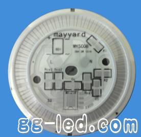
project specification product material Compliance with EU RoHS environmental requirements Main substrate material 96% alumina BaiDu >85% Reflectance >95% Graphic size accuracy ±0.05mm Graphic offset center range ±0.05mm Warpage <0.03mm Substrate surface roughness 0.20-0.75μm Dash depth 40±3% Dam height 0.3 to 0.7 mm Thermal Conductivity 25 W/m. K Thermal expansion coefficient 6.4 to 6.8 ppm/°C Dielectric strength >12KV/mm Volume resistivity >1011Ω.cm (20~300°C) Mechanical strength 350 to 400 Mpa Surface metal layer Sintered silver layer thickness >11μm
 
(2) Specially designed COB light source 1) COB based on material and chip layout design, high thermal conductivity and long service life.
The COB light source part directly mounts the LED light-emitting chip on the ceramic substrate with excellent thermal conductivity. The thermal conductivity of the ceramic substrate is 20 times or more of that of the aluminum substrate. The extremely high thermal conductivity can quickly introduce the heat into the heat sink, and the heat of the LED is The rapid derivation greatly reduces the thermal attenuation of the LED light-emitting chip.
The chip layout of the ring arrangement ensures that each chip has its own horizontal heat dissipation channel, and the scientific and reasonable heat dissipation design truly ensures the high life of the COB light source part. Instead of adopting the centralized series-parallel arrangement mode of the LED light-emitting chip of the usual COB, the middle part of the chip is subjected to more heat, causing the COB to become brighter in the middle part of the light source due to the central temperature concentration after the point is fixed for a certain period of time. Dark light black light attenuation phenomenon. 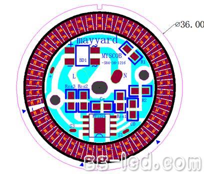
The LED chips are arranged in a double-row annular array, which ensures that the light-emitting channels of each LED chip are more smooth and more unobstructed; the light-emitting surface projected by the LED chip array in a circular layout is softer and the illumination distribution is more uniform. Compared with the equivalent energy COB and point source, the light pollution caused by the point source under the same energy is minimized.
The LED chip is fixed on a high reflectivity ceramic substrate, encapsulated with a high refractive index, low stress silicone resin, and the dam is also packaged with a light transmittance of 80% to minimize light loss, and more fully The light source efficiency is utilized.
3) The LED light source adopting multiple strings and less technology can be driven by a small current, thereby reducing the heat generation of the chip.
The LED light source part is designed to operate in a small current (15-60MA) and high voltage (DC220-256V) mode, which reduces the temperature rise of the LED chip and achieves a perfect match with a low-cost linear constant current driving power supply.
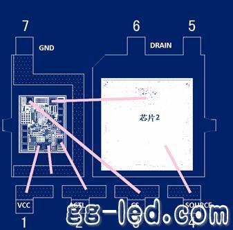
(C) high-voltage constant current drive power <br> <br> using wafer level packaging technology, in an extremely simple circuit structure, to achieve a constant current and high efficiency, and to minimize the power cost. The application circuit of the high-voltage linear constant current driving chip is simple, there is no inductor, transformer and electrolytic capacitor. The principle block diagram of the high-voltage linear constant current driving chip is shown in Fig. 7, and the bare IC is wired as shown in Fig. 8. 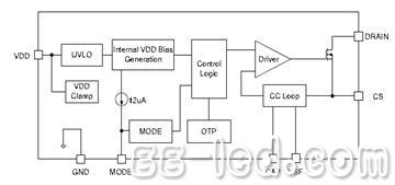
1) Linear segmented constant current LED drive;
2) The LED light string can be automatically switched according to the LED voltage drop;
3) High precision LED constant current (+/- 3%);
4) Maximum LED peak current: 60mA;
5) PFC is as high as 0.99; THD is less than 15%;
6) Automatic current reduction delay life at high temperature;
7) LED open circuit, short circuit, over temperature, VDD under voltage protection;
8) The built-in power tube reduces the number of BOMs;
9) Easily pass EMC test; meet CE, SAA, C-TICK, UL ​​standards;
10) Wafer type packaging.
The bare crystal light engine will become a new generation of LED photo-electricity packaging technology. The bare crystal photoelectric engine will subvert the current LED light source and lamp manufacturing technology. Using the bare crystal photoelectric engine will enable the automated production line to be fast, convenient and simple. The production of bulbs and downlights will greatly reduce the labor cost of enterprises, further reduce the cost of products for LED light sources and lamps, so that LED light sources and lamps have a more intimate retail price, which may become a cheap entry into the civilian population. Blue Ocean LED products.
About the Author:
Author 1: Yan Chongguang Retired Senior Engineer Adjunct Professor of Shanghai Institute of Microelectronics, Peking University 2: He Gangning, Deputy General Manager of Bomeiya Optoelectronics Technology Co., Ltd. 3: Chairman of Wang Yiyue Ningbo Bomei Optoelectronics Technology Co., Ltd. ![]()
Most of Electric vehicle use lead-acid battery bank(12V /6V /8V cells packed in Series)as the power source, The design lifespan of battery is 2~3 years, but actually the battery is usually failure after 6~12 months used which State-of-capacity gradually decline and even some scraped. Through analysis by cutting a large number of failure batteries, the battery water loss and sulfation is quite prominent. Such as the phenomenon of battery sulfation and water dehydration can be effectively inhibited to prolong the service life greatly up to 2 times.
EV Battery Charging Restorer is a new generation of high-tech products developed specifically for restoring Electric vehicle battery when it is charging every time, it utilizes the energy from the charger when charging, generating electronic smart pulse with special frequency to be resonance with the thick lead sulfate crystals in battery charging process. Under the disturbance by the specific frequency pulse, the recrystallization of lead sulfate can be prevented effectively
2. The connection with charger is simple, safe and convenient, and Smart Pulse Charging Restorer can be used in conjunction with the charger for each charging process. The problem of sulfation of the plate can be eliminated during every charging process.
3.It smartly identify 72V/60V/48V/36V battery bank Spec, automatically adapt to precise voltage, automatically adjust the restore electric pulse.This Battery pulse maintainer is suitable for the popular 72V~36V batteries of electric vehicles, buy a set, multi vehicles benefit in family.
4. A strict circuit filtering technique, does not repair your charger as a pulse, without changing the structure of the charger, does not affect the charging parameters of the charger, safe and carefree.
Meiya Optoelectronics: bare crystal engine technology
ã€æ–‡| 颜é‡å…‰çŽ‹ç越何刚】 Integrated package form of LED optoelectronic integrated engine, using wafer form packaging technology, reasonable optical and thermal design, coupled with high-efficiency and high-quality high-voltage linear constant current technology, to achieve optimal optimization A new generation of optoelectronic integrated LED modules with a combination of cost and performance.