O Introduction This article refers to the address: http://
Other Wire To Board Connectors are avialable in different terminations and sizes intended for use on a variety of applications. These connectors provide power and signal with different body styles, termination options, and centerlines. To find the wire to board set required, click on the appropriate sub section below.
Antenk offer Other Wire To Board Connectors like 3.91mm, 3.96mm,4.14mm, 6.2mm, 6.35mm, 10.0mm Available in Male Header, Female Header, Male Housing, Female Housing, Male Terminal, Female Terminal
3.91mm, 3.96mm,4.14mm, 6.2mm, 6.35mm, 10.0mm Wire To Board Connectors Straight type Other Wire To Board Connectors Pcb Board Connectors,Other Wire To Board Connectors,Pitch Wire To Board Connectors,Jst Connector Wire To Board,4.14mm Wire To Board Connectors, 6.2mm Wire To Board Connectors, 10.0mm Wire To Board Connectors ShenZhen Antenk Electronics Co,Ltd , http://www.antenk.com
With the development of technologies such as aerospace and navigation, both on-board and shipboard technical requirements, there is an urgent need for a large-capacity video recording that can work normally in harsh environments (high temperature, low temperature, vibration) and is easy to store. Equipment to meet the requirements of the data management system.
Early massive data records were mainly based on tape drives, but the data stored in the tape drive was kept in a high condition and was susceptible to weather and humidity. The use of a semiconductor memory chip as a storage medium has the characteristics of high storage density, no rotating parts, high reliability, small size, and light weight. Therefore, the semiconductor memory chip has gradually become a mainstream solution for high reliability data recorders.
The large-capacity memory based on the semiconductor memory chip K9WBG08UlM can well meet the requirements of use in harsh environments such as industrial control or military fields.
1 application design of large-capacity memory
1.1 System Composition The entire video compression and large-capacity data storage system is generally composed of a multi-channel video service terminal, a central control subsystem, and a large-capacity electronic storage array. The multi-channel video service terminal is used for collecting and compressing video signals, and the compressed video data is sent to the storage array through the network for storage, and can also be sent to a designated user for browsing through the Ethernet; the central control subsystem is embedded with high performance. The processor BF537 is the core, which can complete the control of the video service terminal and read the storage array data. It exchanges high-speed data with the host computer through 100M Ethernet; the storage array can provide up to 4T storage depth. It consists of 10 independent storage boards with 400MByte capacity, which can provide simultaneous storage services for multiple video service terminals, storage media. The large-capacity non-volatile NAND-Flash chip K9WBG08U1M is used, and the single-chip storage capacity is 32Gbit. Each memory board can be written by the video service terminal and read by the central control subsystem. The block diagram of its system is shown in Figure 1. 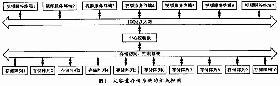
1.2 System working principle After the video signal output by the camera enters the video capture compression card, the video signal is first collected by the A/D converter. After sampling, the digital video signal is processed by the FPGA and then enters the digital signal processor DSP. The video data is video-compressed in the DSP according to the MPEG4 protocol to form a video data stream in the MPEG4 format; the video data stream of each of the acquisition compression boards can be saved to the storage array in real time. If there is a user who needs to access, the data stream is packaged and sent to the specified user.
The compression and storage processes are controlled by the host computer. If there is a user who needs to browse the saved video data, a browsing request needs to be sent to the host computer. After the host computer accepts, the data block in the storage array can be selected by reading the data logic, then read out, packaged and sent to the designated data. user. The master computer can respond to requests from multiple users simultaneously.
2 large-capacity electronic storage array design
2.1 Data Transceiver Interface The data transmission and reception of the storage board can be realized by DSP. Considering the consistency with the front-end chip selection, this solution selects the ADSP-BF533 of Analog Devices as the data transceiver processor. When performing a store operation, the BF533 will receive the memory data sent from the central control board from the input/output bus parallel peripheral interface (PPI) and buffer it into the SDRAM. At the same time, according to the programming timing requirements of the K9WBG08U1M, the memory programming instructions are formed. The FPGA sends the K9WBG08U1M memory chip; when performing the read operation, the BF533 sends a read operation instruction to the K9WBG08U1M through the FPGA to read the data of the specified area and cache it in the SDRAM memory, and then send it to the SDRAM through the input/output bus (PPI). The center controls the subsystem and sends it back to the host computer for browsing.
2.2 Memory Access Control Interface The access control interface of each memory board can be implemented by two FPGAs. Since there are 100 memory chips K9WBG08U1M on the board and only one set of input/output buses, access to the chips needs to be realized by bus driving and decoding logic. This logic can be implemented by ALTERA's Cyclong series FPGA, the specific model is EP2C35F67218, which can also exchange data with DSP through EBIU bus. The data written or read by the memory chip needs to pass the EP2C35. Since there are 100 memory chips on the board connected to one set of I/O pins of EP2C35, the load will be too large to work. Therefore, the memory chips can be grouped in groups of 4 and share a set of EP2C35 I/. The O pin is driven to ensure sufficient drive capability. The address signal from the bus is input to an address decoder for selecting a memory chip. The input is a 7-bit address line, and the output memory chip selection signals csl to csl00 are connected as shown in FIG. 2 . 
3 File Management Because the storage array has a storage depth of 4TB, the file length and compressed file size are not fixed. Therefore, according to the inherent characteristics of the Flash device, a FAT file system suitable for managing NAND Flash memory can be constructed. And by improving the storage mode of the FAT table to extend the life of the memory and improve the stability of the system storage. However, it is therefore necessary to manage the video files taken for each task. To this end, a simple file recording system can be designed in the system, including file name, storage address, file size, corresponding camera number, shooting time and duration. The recorded information can be saved in the FAT entry area of ​​the FLASH for basic file management operations such as deletion, copying, cutting, downloading, array formatting, and the like.
3.1 File Write When the central control subsystem receives the start shooting command, it can send a start command to the front-end video capture system through the network, and send a start command to the storage array according to the corresponding relationship between the camera number and the storage array. The storage array is created. After the file index table entry, it waits to receive the video data until the central control subsystem receives the end command sent by the host computer, and then writes the file name, file length and other related information, thereby completing a file writing process.
3.2 File Download When a user needs to browse the file information stored in the storage array, the host computer can send a browse command to the central control subsystem. The central control subsystem sends a browse command according to the protocol between the storage array and the storage array, and the storage array obtains the saved video file record information from the memory and generates a file list, and then packages it back to the central control subsystem, and then sends it back according to the FIP download format. The upper computer displays that the user can select a file to perform a download operation according to the returned information list. In order to match the download speed and the network transmission speed, this paper designs a download mode with flow control so that the download speed can be completely controlled by the central control subsystem.
3. 3 File Management In fact, NAND Flash memory sometimes has bit reversal, and there may be bad cells in use. Therefore, data writing must be performed in a blank block or an erased block. The underlying technology requires erasing in blocks and then writing by page. If there is useless video data in the storage array, the user can select the corresponding file as needed, extract the address parameters of the file storage, and then delete the file. Considering the life of the storage array, the probability of using each chip is about equal. The design uses a sequential storage format to store files. However, when the file is deleted, a large amount of unused blank areas are left in the storage array, so that the storage array usage is greatly reduced. For this purpose, the storage array file sorting function and formatting function can be designed in the storage array. When the proportion occupied by the blank area is high, the host computer sends a file sorting command to the central control sub-system, so that the central control sub-system controls the storage array to perform the file sorting operation, and returns the delivery status to the upper computer after finishing the finishing. For storing more important files. File copy commands can be used to back up files between several storage arrays to improve system reliability. In a storage array, when the useful file share is small but there are many files, the valid file can be copied and the storage array can be formatted.
4 Conclusion This design is convenient and flexible, and can be used for designing high-speed, large-capacity, high-reliability electronic storage devices. In fact, for the system that requires large capacity, high reliability, and harsh operating environment, the system designed in this paper can meet the initial expected effect well, and has been applied in a certain type of system.
3.91mm, 3.96mm,4.14mm, 6.2mm, 6.35mm, 10.0mm Wire To Board Connectors Right Angle type
3.91mm, 3.96mm,4.14mm, 6.2mm, 6.35mm, 10.0mm Wire To Board Connectors Male Housing
3.91mm, 3.96mm,4.14mm, 6.2mm, 6.35mm, 10.0mm Wire To Board Connectors Female Housing
3.91mm, 3.96mm,4.14mm, 6.2mm, 6.35mm, 10.0mm Wire To Board Connectors Male Terminal
3.91mm, 3.96mm,4.14mm, 6.2mm, 6.35mm, 10.0mm Wire To Board Connectors Female Terminal