LCD Technology Trend Analysis Table 1 LCD technology development projects Most need: â—Ž, need: O, second: D Table 2 Manufacturer's high-resolution LCD Table 3 Various types of wide viewing angle technologies Note: MVA (MulTI-domain VerTIcal Alignment); Super-IPS (In Plane Switch) 4. Response speed LCD-TV most requires animation to show the effect, so LCD response speed is a key issue. With NTSC display mode and 60Hz display frequency, each Frame is only 16.7ms. The current laptop computer panel specifications are mostly 30 ~ 40ms. If the LCD response speed is too slow, the image will have image sticking defects. For TN Mode liquid crystal materials, the response time is proportional to the liquid crystal rotational viscosity, the anisotropy of the induced rate, the applied voltage, and the square of the cell pitch. So manufacturers must look for low viscosity liquid crystal materials, but low viscosity liquid crystal materials will affect other characteristics, In order for the light source to be evenly distributed to the panel, the LCD must have a random function structure. Therefore, reflective LCD technology is roughly divided into Diffusing Reflector Type (diffused reflector type), Front Scatting Type (scattered front panel type) and Scattering Reflective LCD plus reflective plate will block the light of the backlight module, so the only light source required for the LCD panel is the natural light source and the front light source. The front light source is a white linear light source, placed on the side, and diffused into a uniform surface light source by the light guide plate. Above the light guide plate of the front light source (on the user's side), special processing is needed to form a V-shaped groove or stepped groove nest (Figure 2) to reduce light leakage during the light guide process, but the light passing through the LCD panel must penetrate. The anti-reflection film should be designed under the light guide plate so that the light guide can enter the LCD. Led Street Light,Led Street Lamp,Solar Led Street Light,Solar Street Lamp Post Jilin Province Wanhe light Co.,Ltd , https://www.wanhelight.com
Foreword LCDs with the advantages of light and thin, power saving, and no radiation, due to the larger size and better product specifications, the market has been continuously expanded. However, the fierce competition caused by this makes manufacturers have to constantly innovate in technology in order to continue to stimulate the market. For technology development, there are actually only two purposes: to reduce costs and improve performance. Therefore, LCD manufacturers have begun to develop technologies in three aspects, including panel design, factory production line manufacturing improvement, and application product matching. In addition, how to achieve the CRT's wide viewing angle, high contrast, high-speed response, color performance and other qualities, and even strengthen the LCD's lighter, thinner, power-saving, high-resolution characteristics
To consolidate existing areas and prevent other technologies from replacing, it is also the goal of manufacturers to continuously strive to improve. Therefore, this article explains these technical trends. 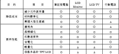
Source: PIDA
As can be seen from Table 1, the LCD technology required for different application products is not the same, and manufacturers must develop suitable products for their key markets. But the only same requirement is to reduce costs, because more and more competitors, even new display technology products will be born, LCD manufacturers must continue to reduce costs to consolidate the market.
Generally speaking, the easiest way to reduce costs is to transfer the back-end project to a place with low labor cost. However, the labor cost only accounts for 10% of the total cost. The real key lies in the material that accounts for 50% of the cost. How to reduce the use of materials, in the long run, must start with the improvement of materials and processes.
According to the survey results of the MRI entrusted by the Information Promotion Team of the Ministry of Economic Affairs, and the technical achievements of various manufacturers in displaying new products,
To reduce costs, different methods must be used in different process stages. Although the key to the cost of TFT Array lies in the equipment and the process itself, the material cost of other process steps seems to be quite high. Therefore, the first stage of the cost reduction method includes the improvement of the Array process through equipment, reducing the number of masks and reducing the exposure steps, shortening the process time and increasing output; the cell section project has the lowest yield, and the improvement of yield is the key; the module section Engineering, the backlight module is the key material, but currently the backlight module forms a surface light source by light guide, which requires many optical components.
Not only the cost is high, but also the weight and space are increased. The new technology is to micro-machine the light guide plate to produce a prism function, saving optical film and reducing the structure.
After such improvements, the first stage goal can reduce costs by 36 to 46%.
In the second stage, considering that the equipment investment is too expensive, I hope to use the same equipment to shorten the TACT TIME of each process to increase production. On the other hand, new process concepts such as Color filter are used on the TFT substrate, and the driver IC is integrated in the glass. The goal is to reduce the cost of materials. The second stage aims to reduce costs by 22%. In short, manufacturers aim to reduce costs by 60% in 2003, and achieve the goal of 1.5 times the price of LCD panels for CRTs, and therefore are expected to replace the 40% CRT Monitor market. However, this "ideal" obviously needs the cooperation of upstream manufacturers to have a chance to succeed.
According to the survey, between 12.1 inches and 14.1 inches, LCD panel manufacturers provide nearly 300 specifications, and the materials used to produce the panels are more complex than the stars. And because there is no certain standard to regulate, notebook computer manufacturers are quite troubled when purchasing,
It also makes the preparation of LCD manufacturers very tricky, which will inevitably lead to increased product costs. So Compaq, IBM, DELL, HP, Toshiba
Manufacturers form SPWG (Standard Panel Working Group) to develop standardized standards for notebook computer panels 13.3, 14.1, and 15 inches. Although Standard 1.0 and 2.0 have been released, there are still unstandardized items such as thickness, weight, response speed, brightness, and electronic signals. At the same time, although setting standards can help LCD manufacturers reduce costs, many manufacturers have introduced various new specifications to grab card slots under the market's swindles, making it difficult to implement the ideal of unified standards. However, there are actually some standards that allow LCD
The factory and the notebook computer factory follow the design.
Improve performance
1. Thin and lightweight portable products are often advertised as thin and light. Taking notebook computers as an example, LCD accounts for 18 ~ 25% of the weight of notebook computers, which is the heaviest component, which makes it lighter to reduce the weight of LCD. The most important subject. LCD manufacturers plan to reduce the weight of 14.1-inch panels from 560 grams in 2000 to 420 grams in 2002, and the thickness from 6mm in 2000 to 4.7mm in 2002. This improvement is more than 20%.
If we discuss the overall weight of LCD components, the glass substrate is the largest part, about half, followed by the backlight module, accounting for 41%. Therefore, in order to achieve the goal of light weight, glass substrate manufacturers need to provide thinner substrates, starting from 0.7mm, which is the most commonly used now, and moving towards thinner and lighter. Taking Coring's Eagle 2000 as an example, the density is reduced from 2.54 g / cm3 to 2.37 g
/ Cm3, the thickness is reduced from 0.7mm to 0.63mm, so that the weight can be reduced by 13%. As for the backlight module, the backlight module is composed of many optical structures, and using a lighter material light guide plate will be an immediate solution. The light guide plate material is replaced by transparent acrylic resin with light-scattering resin material, and the light guide plate is finely processed into grooves to replace optical thinness. This will not only reduce the thickness and weight, but also reduce the price. The direction of efforts. In addition, some manufacturers have come up with a direct light source to replace the complex light guide structure, although the idea is good, but the price is not low.
2. High resolution As the size of LCDs continues to rise, high resolution becomes another battlefield. 13.3-inch notebook since 1999
After the mainstream PC size, XGA resolution replaced the mainstream status of SVGA, and after 14.3 inches squeezed out 13.3 inches in 2000, XGA
The proportion of resolution in the market is as high as 70%, which has caused SXGA + and UXGA to show their faces at the end of 2000. LCD Monitor
In general, XGA is still the mainstay. With the proportion of more than 15-inch products exceeding 20% ​​in 2001, large-scale panels driving SXGA and above resolution will gradually become the mainstream, and even 2005 UXGA (1600 × 1200) is expected to become the most Bulk choice.
As for TV, the focus of the request is on the picture rather than the text, so the resolution SVGA is sufficient to meet the current TV requirements. For example, NEC shipped a LCD-TV with a resolution of only VGA for 20.1-inch TVs at the end of 2000. However, since the LCD-TV market is still in its infancy, the resolution of multimedia wide-screen TVs is mainly XGA ~ WXGA (1280 × 768), SHARP 28 inches
LCD-TV is WXGA. Samsung Electronics Co., Ltd., which is actively entering LCD TVs, will use WXGA ~ UXGA of 24 ~ 32 inches in 2002
For product planning, but with HDTV as the appeal in 2005, a 40-inch large TFT LCD with a resolution of 1920 × 1080 pixels is required.
When the resolution is higher, the RC delay on the circuit will cause the GATE signal to deform, and the pixel data writing time is not enough, resulting in poor brightness contrast. Therefore, in order to achieve a high-definition picture, the bus line resistance and parasitic capacitance must be reduced. Choose Cu, Al-based low-resistance metals, or Mo / Al, Ta / Al, Cr / Al-based laminated structures can be used as Gate Bus Line to reduce the Bus line resistance. In addition,
It is also a good method to reduce the overlap between Source and Gate to reduce the parasitic capacitance. Of course, high-resolution products will make the screen more detailed, but it makes the LCD aperture ratio relatively lower, which forces the backlight brightness to be increased to give users the same brightness screen, and it also increases power consumption. Therefore, in addition to improving the light source design of the backlight module and improving the efficiency of the Invertor, the LCD manufacturers also need to improve the process to increase the aperture ratio. In addition, the increase in signal frequency due to higher resolution
EMI problems, as well as temperature rises caused by increased relative circuit power consumption, make heat dissipation and EMI another thorny issue.
In addition to the hardware and process technology issues, in software, the resolution of the LCD must be matched with the computer operating software. Because the resolution is too high, the font is too small and the visibility becomes poor. Window2000 will solve the problem caused by fixed font points. The attached table shows the best display resolution for panels of various sizes. Generally speaking, 120ppi is already the limit of human eye recognition.
3. The wide viewing angle LCD uses the liquid crystal rotation to control the light, which causes the shortcomings of congenital narrow viewing angle. When faced with a large LCD screen, the problem of wide viewing angle becomes obvious. In the past, the most convenient method was to attach a wide viewing angle film. However, the wide viewing angle film is an exclusive material of FujiFilm in Japan, and the cost is not cheap. Therefore, various LCD factories have developed new liquid crystal materials and new structures to improve the liquid crystal alignment and enhance the viewing angle. The technologies that have been successfully applied to the volume products include Fujitsu ’s MVA technology and Hitachi IPS technology. In addition, in recent exhibitions, other manufacturers ’new technologies, such as Samsung Electronics’ PVA (Patterned VerTIcal Alignment) and modern FFS (Fringe Field Switch) technologies , Can achieve a viewing angle of 170. .
Among them, Fujitsu MVA technology is a combination of vertical alignment (VA) mode liquid crystal and multi-domain method. VA liquid crystal is arranged vertically,
The optical characteristics are less affected by the viewing angle. The multi-domain method divides each pixel into several sub-pixels, and each sub-pixel has its twisted arrangement and viewing angle characteristics. As long as the sub-pixel position allocation is designed properly, the viewing angle characteristics of each sub-pixel complement each other, and the angle of view becomes wider and non-directional after synthesis.
Therefore, Fujitsu uses the design of bumps on the glass substrate to control the arrangement of liquid crystal molecules, so that the conventional rubbing can be omitted (Rubbing)
Alignment process to reduce particle pollution caused by alignment. However, in order to improve the aperture ratio, increase the light transmittance, and reduce the bump process steps, Fujitsu designed a new MVA structure, using ITO pores as a virtual bump effect, which can reduce light leakage and increase the aperture ratio by 10%.
The contrast also changed from 300: 1 to 500: 1. Because Fujitsu takes large-scale business curtain products as its product strategy, it has actively developed mass production technology with a wide viewing angle. At present, Fujitsu has started mass production of 15-inch XGA and 17.4-inch SXGA TFT LCD with new MVA structure, and 23.1-inch UXGA has also started mass production with 160 viewing angles. , The response speed is below 25ms. 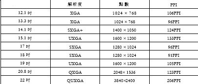

ASV (Advanced super View); OCB (Optical Compensated Birefringence)
The Korean Samsung PVA technology also uses a vertical alignment mode liquid crystal material, using ITO electrodes designed on the upper and lower two pieces of glass.
Fringe filed is formed on the edge of the electrode, and the multi-domain effect is achieved with the compensation film, and the viewing angle is also widened. Samsung said that this method is compatible with the original process and has a high penetration rate.
As for the Hitachi IPS liquid crystal mode, regardless of the state of the electric field, the liquid crystal molecules only rotate in the horizontal direction, so even if the gaze position changes,
The optical characteristics also rarely change, so the viewing angle range is increased. This mode controls the liquid crystal electrodes to be designed on the same plane, mainly to generate a horizontal electric field to control the liquid crystal molecules to rotate in the horizontal direction. However, due to the IPS structure design, there are still some disadvantages such as tone inversion, poor contrast, and white shadows. Therefore, Hitachi added a new structure of multiple-domain compensation, called Super-IPS, to improve For the above shortcomings, the comparison has also been increased from 200 to 350. At the same time, Hitachi uses new liquid crystal materials and improves the driving effect to increase the IPS response speed to 30ms. At present, Hitachi has started mass production perspective 170. 15, 18.1 inch SUPER-IPS TFT LCD, and in 2001 can measure 19 inch new products. Hyundai Electronics has developed FFS wide viewing angle technology similar to IPS, forming a fringe electric field (FringeFiled) with a narrow pitch between the upper and lower plates to achieve a multi-domain effect, and using negative liquid crystal materials and replacing metal electrodes with ITO electrodes to achieve higher light transmittance. But FFS structure requires more processes than IPS.
The manufacturer must adjust the optimized materials in the dilemma. Reducing the distance between the two LCD substrates is also a method to speed up the reaction time, but too narrow a distance may cause problems such as electrode short-circuiting and liquid crystal filling time is too long, affecting the yield.
In 1993, the OCB (Optically Compensated Birefringence) mode proposed by Professor Uchida of Tohoku University in Japan, the liquid crystal molecules on the upper and lower substrates are arranged in parallel, and the inner molecules are not twisted but only bent. Therefore, to control the light, the liquid crystal molecules need only be changed Achievable, the reaction speed is much faster. Panasonic exhibited a 7-inch TFT LCD in OCB mode for 7ms in 1999.
In 2000, the 15.2-inch TFT LCD in OCB mode was developed in only 3ms. However, Panasonic said it is still under development, and mass production will take some time, but Sharp has planned to mass-produce 15ms LCD-TV panels in the second quarter of 2001.
5. Reflective technology generally penetrates LCD power consumption, 90% of STN and 70% of TFT power comes from the backlight. To reduce LCD power consumption,
Reflective LCDs that do not require a backlight become a good choice, and they must be the future trend. In the traditional reflective LCD, a scattered reflective plate is added to the outside of the glass substrate on the back side of the transmissive LCD. This method does not need to change the structure of the original LCD, so the cost is low and mass production is convenient, so it is widely used in low-resolution products, such as watches, computers and other products. However, because the glass has a certain thickness, the incident light and the reflected light are different through the pixels, causing parallax, resulting in a decrease in contrast and color purity. In order to solve the shortcomings of parallax, the high-resolution color reflective LCD uses a structure in which a reflective plate is placed inside the glass substrate. 
Three types of LC Type (scattered liquid crystal), as shown in Figure 1. The diffuse reflection plate type is easy to obtain a uniform viewing angle, but the process is more complicated; the front scattered plate type process is simpler, and local higher contrast and brightness can be obtained, but the control of the viewing angle is slightly more difficult. The scattered liquid crystal type uses materials with light scattering characteristics, such as PC type (Phase Change) or PDLC (Polymer Dispersed Liquid Crystal) type liquid crystal, to complete the scattering mechanism, but has the disadvantages of insufficient light scattering effect and higher driving voltage. 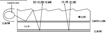
Recently, several new mobile phones with TFT LCD have been introduced, and the front light source has been adopted. At present, the reflective type has been applied to small and medium-sized products such as 4 to 8 inches (such as PDA, game instruments, etc.). It still needs to work on the characteristics of brightness and contrast. The long-term goal is to achieve the visual experience of general paper prints.
Conclusion Under the pressure of declining prices, Japan, the leader of the liquid crystal industry, has to step up its efforts to develop display components suitable for various applications in order to open up new markets. Even six Japanese LCD manufacturers such as Sharp have invested in the establishment of a technology development center. To develop basic technologies for energy-saving processes, prepare in advance in response to strict environmental protection requirements in the future.
In recent years, LCD technology has advanced by leaps and bounds, and the rendering effect has reached the realm of CRT. Therefore, it is estimated that the LCD market value in 2003 will take away the CRT championship for the first time. In order to achieve the largest market for printed displays that replace the real world, LCD still has some way to go. Taiwan's LCD industry is already the top three countries in the world, and it needs to understand the technological evolution and be at the forefront of technology to develop this large industry in the long run.