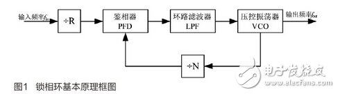
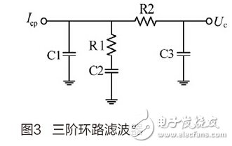
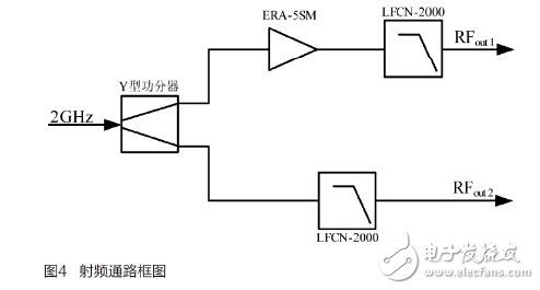
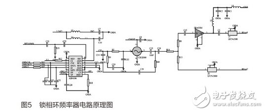
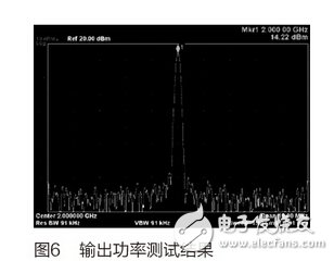
introduction The function of the frequency synthesizer [1-2] is to provide a frequency-programmable local carrier signal to the frequency conversion circuit in the transceiver. It is one of the core modules of the wireless transceiver, and its performance has a significant impact on the communication quality of the communication system. At present, the frequency synthesizer mainly has four kinds of implementations: direct analog frequency synthesis technology (DS), phase-locked loop frequency synthesis technology (PLL), direct digital frequency synthesis technology (DDS), and hybrid frequency synthesis technology. The phase-locked loop frequency synthesizer It is the most commonly used structure in RF circuits. Compared to several other structures, the PLL structure can synthesize high-performance carrier signals with limited power consumption. This paper designs a digital phase-locked loop frequency synthesizer based on phase-locked loop chip ADF4106, which has wide bandwidth, good noise characteristics, fast locking time, low power consumption and small size, so it is widely used. In a wireless communication system. 1 Basic working principle of phase-locked loop frequency synthesizer The phase-locked loop (PLL) is a phase error control system that compares the phase between the input signal and the voltage-controlled oscillator (VCO) output signal to produce a phase error voltage that is processed to adjust the phase of the voltage-controlled oscillator. When the loop is locked, the frequency difference between the input signal and the voltage controlled oscillator output signal is zero, and the phase difference no longer changes with time. At this time, the error control voltage is a fixed value, and the output frequency of the voltage controlled oscillator is equal to the input signal frequency. That is, fout=(N/R)*fin. The basic principle block diagram of the phase-locked loop is shown in Figure 1. The main structure of the phase-locked loop consists of a VCO, a phase detector (PFD), a frequency divider, and a loop filter (LPF). Among them, the main function of PFD is to compare the phase. It divides the VCO output signal by N and compares it with the input frequency R to generate an error control voltage. The role of the LPF is to filter out high frequency components and noise in the error voltage to ensure the required performance of the loop and improve system stability. The VCO is controlled by the control voltage so that its output frequency approaches the frequency of the reference signal, and the difference between the two frequencies becomes smaller and smaller until the frequency difference is eliminated and the phase synchronization is locked. In the actual design, the division ratios R and N can be changed by the program to obtain the required stable output frequency. 2 program design and implementation 2.1 Phase-locked loop chip ADF4106 structure function introduction The ADF4106 is an integrated phase-locked loop frequency synthesizer chip from Analog Devices, Inc., which enables local oscillation of the upconversion and downconversion sections of the wireless transceiver. The ADF4106 consists of a low noise digital PFD, a precision charge pump, a programmable reference divider R (14 bits), a programmable A (6-bit), B (13-bit) counter, and a dual-mode prescaler. P/P+1 composition. The A and B counters are connected to the dual-mode prescaler to implement a divider N, and N = PB + A. The chip has a frequency bandwidth of 6GHz, a supply voltage of 2.7V~3.3V, independent charge pump supply voltage, programmable dual-mode prescaler P/P+1, and its value can be 8/9, 16/17 32/33 and 64/65, with three-wire serial interface, analog digital lock detection, hardware and software low power mode. The ADF4106 can form a complete PLL circuit with the external LPF and VCO. The wideband nature of the ADF4106 eliminates the use of frequency multipliers in many high frequency systems, simplifying system architecture and reducing cost. In the design of this paper, a 2GHz frequency synthesizer is designed, and the 2GHz frequency signal is required to be divided into two outputs, and one of the output signal powers is guaranteed to reach 13dBm. The circuit is mainly composed of ADF4106, LPF, VCO and RF signal output part. According to Figure 1, the input signal frequency is selected to be = 10 MHz, and the signal is impedance matched by a T-type matching network before entering the Refin pin of the ADF 4106. In order to ensure that the PFD input signal frequency is 1MHz, it is necessary to programmatically set the value of the reference divider R to 10 and the value of the divider N to 2000. The ADF4106 has a simple SPI-compatible serial interface that writes data to the device pins CLK, DATA, and LE. When LE is on the rising edge, the 24-bit data stored in the register on each rising edge of CLK is fed into the appropriate latch. In the device. The serial input timing diagram is shown in Figure 2. 2.2 LPF design LPF directly affects the phase noise and switching frequency of the frequency synthesizer during the design of the frequency synthesizer. Since the output of the PFD includes not only the DC control signal but also some high-frequency harmonic components, the LPF performs appropriate parameter setting on the resistor and capacitor. It can filter out high frequency components and avoid these harmonics from affecting the next stage VCO circuit. LPF can be divided into active filter and passive filter. The passive LPF designed in this paper converts the charge pump output current into control voltage and suppresses the output ripple of phase-detection frequency. In the circuit design process, since the second-order LPF is difficult to suppress the ripple of the loop bandwidth frequency by more than ten times, the third-order LPF [3] is used to improve the suppression of the spurious frequency. The circuit diagram of the third-order LPF is shown in Figure 3. For the values ​​of the capacitance and resistance in the LPF, the ADS of the LPF simulation software ADIsimPLL provided by Analog Devices (ADI) and the ADS of Agilent (Note: now known as Keysight) The simulation software is simulated. By setting the relevant parameters and continuously optimizing and debugging, the parameters of each device of LPF are: C1=100pF, C2=1.5nF, C3=20pF, R1=4.3kΩ, R2=6.2kΩ . 2.3 VCO function introduction As a voltage-to-frequency converter, the VCO plays an important role in the PLL because it can produce the final output signal frequency. The VCO is a frequency-modulated oscillator with linear control characteristics. Its output frequency changes with the change of the control voltage, so that the output signal frequency approaches the frequency of the reference signal until the frequency difference is eliminated. VCO [4] has device characteristics such as phase noise, frequency stability, frequency range, and harmonic suppression. In this paper, considering the design index requirements, Z-CommunicaTIons CRO2000 is selected as the voltage controlled oscillator. Because of its low phase noise, good harmonic suppression, good linearity and easy soldering device package, The device was chosen as the VCO of the PLL and achieved good performance in practical applications. 2.4 RF channel design Since the VCO output load impedance is 50Ω, the 2GHz output signal RF trace impedance [5] is also required to be 50Ω. The printed board of this paper uses a lamination method, in which the first layer of dielectric material is Rogers4350B, the board thickness is 20mil, and the dielectric is dielectric. The constant is 3.48, and the RF trace width is 40 mils calculated by the simulation software Polar Si9000. The RF path design block diagram is shown in Figure 4. This paper requires 2GHz frequency signal to be divided into two outputs through Y-type resistive power splitter, and ensure that one of the output signal power reaches 13dBm. Since the VCO output signal power is small, it is necessary to add an amplifier ERA-5SM to the path to ensure the output power value, and in order to suppress interference such as harmonics and non-harmonics outside the 2 GHz signal, it is necessary to add low at the output of the two paths. Pass filter LFCN-2000. 2.5 Phase-locked loop frequency circuit schematic and test results Based on the introduction and design of each module of the phase-locked loop frequency device described above, the final circuit design is shown in FIG. 5. According to the schematic diagram shown in Figure 5, the corresponding PCB external processing is drawn, and the processed printed board is installed into the shield box designed in advance to test. The test results of Agilent N9020A are shown in Fig. 6 and Fig. 7. Figure 6 shows the output signal power test results, and Figure 7 shows the phase noise test results. As can be seen from Fig. 6, the power at the output signal of 2 GHz is 14.22 dBm, which satisfies the requirement that the signal power reaches 13 dBm. At the same time, as shown in Fig. 7, the single-sideband phase noise of the output signal is -103.136dBc/Hz@10kHz, which also satisfies the design index. 3 Summary Frequency synthesizers play an important role in modern communication systems, and their performance determines the performance of communication systems. The frequency device designed based on the phase-locked loop chip ADF4106 has the characteristics of low noise, low power consumption, low cost and simple circuit structure, and thus is widely used in the field of wireless communication systems.
Glass Bowl Food Choppers are our main food choppers. We have 0.6L, 1.2L, 1.8L optional with pure clear and thick glass bowl. Besides, we have molding polyfoam packing for glass bowl and our glass bowl is thick and strong, it is not easy broken. What's more, glass bowl is easy to clean.
Description of Glass Bowl Food Choppers
300W/350W
S/S housing
pure clear and thick glass bowl with double blades
one/two speeds with safety lock
metal gear
6pcs/ctn
Glass Bowl Food Choppers Glass Bowl Food Choppers,Glass Bowl Choppers,Kitchen Food Processor,Vegetable Chopper Flying Electronic Co., Ltd , https://www.flyingelectronic.com