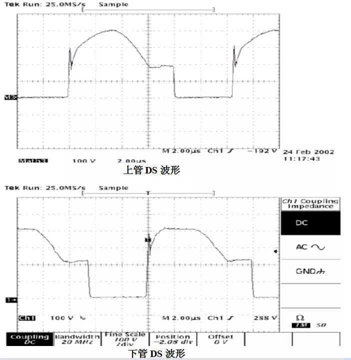
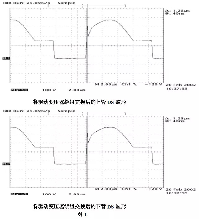
The double-tube forward circuit has high reliability, and this form of lossless absorption circuit also has a better effect on improving the switching trajectory of the upper and lower power tubes. Let's analyze the working process of the circuit first: Let's first understand its working process analysis Suppose the initial working state of the circuit is that the switch tube is off, and the secondary side of the transformer is in a freewheeling state. At this time, the upper and lower pipes are opened at the same time, then the circuit will go through the following processes The junction capacitance of the stage 1 tube can be generated to zero at the moment when the tube is turned on. The 410V DC bus voltage is added to the resonance network composed of C23, VD30, L5, VD29, and C22 to form series resonance. Due to the reverse resistance of the diodes VD29 and VD30 The off action makes the final resonance result that the voltage on C23 and C22 remains at the bus voltage of 410V. In stage 2, the upper and lower tubes are turned on, and the current flows through the primary side of the transformer to provide energy to the load. Stage 3, after the duty cycle D is turned on, the power tube starts to turn off. At this time, the load current still flows through the primary side of the transformer, so in the initial turn-off stage The high current of this load charges and discharges C22, C23 and the junction capacitance of the tube linearly. During this process, the sum of the voltage on the junction capacitance of the lower tube and the voltage on C22 is always maintained at 410V, and the voltage on the junction capacitance of the upper tube is also the same as that on C23. The sum of the voltages is 410V, and the voltage on the primary winding of the transformer drops accordingly. At this point, a complete work cycle is over. Causes of wave asymmetry The above is an ideal analysis of this circuit. The DS waveforms on the upper and lower power tubes should be completely symmetrical. But in fact, due to the discreteness of the device parameters, the driving of the upper and lower tubes, and the inconsistency of the wiring, the DS waveforms of the upper and lower power tubes will have a large deviation, which is manifested as an early DS voltage when a tube (for example, the lower tube) is turned off. It rises and clamps at the bus voltage, and at this time the resonance envelope of the upper tube is far from reaching the bus voltage. As shown in Figure 2 below: The simplest intuitive explanation for this phenomenon is that the currents flowing through the upper and lower resonant branches are different from the time the tube is turned off. The reason for this difference comes from the inconsistency of the turn-off time of the upper and lower power tubes, that is, when a tube is turned off. When the current has decayed to zero, there is still current in the other tube. In this way, the capacitors on the upper and lower resonant branches will accumulate different charges and generate different voltages. This will naturally lead to inconsistent resonance waveforms of the upper and lower tubes. In order to verify this, take a picture of the DS waveforms when the upper and lower two tubes are turned off for comparison (Figure 3) The upper waveform corresponds to the turn-off of the lower tube, and the lower waveform corresponds to the turn-off of the upper tube. It can be seen from the waveform that the turn-off of the lower tube is indeed faster than that of the upper tube. In order to continue the verification, the two sets of drives of the drive transformer are switched up and down. From the experiment, it can be seen that the DS waveforms of the upper and lower tubes are almost completely symmetrical. A small resistor is appropriately connected in series in the reverse pumping loop of the down tube drive to reduce its turn-off speed. The same result can be obtained, and the waveform is shown in Figure 4. So far, it can be said that the power tube has asymmetrical waveforms of the upper and lower tubes due to the inconsistency of the turn-off time. The solution to the problem of asymmetry of waveform The impact of this phenomenon on the normal operation of the circuit is that if the waveform is severely asymmetric, the energy accumulated on the DS junction capacitance of the upper and lower power tubes will be very different when the upper and lower power tubes are turned off, and the clamp diode with the smaller energy will not participate at all. It works, but the energy-rich one will feed energy back to the DC bus through the clamp diode for a long time, causing the diode temperature to be high and the reliability drops severely, and the diode will be damaged. Therefore, it is necessary to reduce its asymmetry to a certain range. . The solution is to adjust as much as possible to make the turn-off time of the upper and lower tubes consistent. Therefore, the upper and lower tubes should be as symmetrical as possible during PCB wiring, and the two drive windings should be as consistent as possible when winding the transformer. And under the condition that the PCB board, drive transformer, and drive parameters have been established, the asymmetry is also fixed. For example, the voltage of the lower tube is high and the voltage of the upper tube is low, but the degree of asymmetry is slightly different. Put a small resistor in the drive anti-pumping circuit of the fast turn-off speed to artificially reduce the turn-off speed to synchronize with the other way, but doing so will affect the efficiency of the whole machine and increase the temperature rise of the power tube. Therefore, a compromise must be considered. Some also take the method of increasing the transformer magnetizing inductance to solve this problem. I understand that this method does not solve the fundamental problem. It only increases the excitation energy, so that the energy of the upper and lower tubes is accumulated to a certain extent, which makes it clamped. The diodes are all turned on, which is equivalent to forcibly pulling the waveform symmetrical and does not reduce the burden of the clamp diode. And the corresponding increase in leakage inductance will also extend the dynamic conversion time.
USB Cable :1.Type A: almost every USB cable has a standard flat rectangular interface at one end. Most computers have a usb-a port to connect to only one USB port.
2.Type-B: almost square connector for printers and other active devices connected to computers. They are not common now because most devices have been moved to smaller connections.
3.Mini USB: a smaller connector type that was standard for mobile devices before micro USB. It's not common today, but you'll see it on some cameras, PlayStation 3 controllers, MP3 players, etc.
4.Micro USB: the current standard for mobile and portable devices, even smaller than Mini USB. Although you can still find micro USB on smartphones, tablets, USB battery packs and game controllers, some have turned to usb-c
5.Type-C: the latest USB standard, which is a reversible cable, promises higher transmission speed and higher power than previous USB types. It can also take into account a variety of functions.
USB Cable ShenZhen Antenk Electronics Co,Ltd , https://www.antenkcon.com
Due to the linear charging and discharging effect of the load and the large current, the maintenance time of this stage is very short. As a result, the upper and lower tube junction capacitances and the voltages on C22 and C23 are all about 205V. Phase 4 From this moment on, since the voltage of the primary side of the transformer has dropped to zero, the secondary side freewheeling diode begins to conduct, and its current gradually increases, while the current on the rectifier diode gradually decreases. At this stage, the rectification and freewheeling diode are at the same time When the transformer is turned on, the voltage on the secondary side of the transformer is clamped at zero, and the voltage on the excitation inductance of the primary side of the transformer is also maintained at zero. The leakage inductance of the transformer resonates with the junction capacitance and the absorption capacitor. The voltages on capacitors C22 and C23 are reduced accordingly to maintain their sum at 410V.
When the primary current drops from the load current resonance to the excitation current, the secondary rectifier diode is turned off to end the commutation. However, due to the reverse recovery of the diode, there will be several cycles of repeated oscillations on the primary side leakage inductance until the rectifier diode is completely turned off. At this time, only the excitation current flows through the primary side of the transformer because this period of time is also very short. Therefore, there is almost no attenuation of the excitation current. In stage 5, the excitation inductance on the primary side of the transformer resonates with the junction capacitance and the absorption capacitor. The excitation current continues to charge and discharge the capacitor so that the voltage on the junction capacitor continues to oscillate and rise with a larger resonance period, and the voltage on the absorption capacitor continues to decrease, but Since the absorption capacitance is much larger than the junction capacitance, the resonant current mainly flows through the absorption capacitance, which makes the absorption circuit have a better absorption effect on the power tube.
If the energy stored in the magnetizing inductance is relatively large, the resonant voltage on the power tube will exceed the bus voltage of 410V. At this time, the clamping diodes VD27 and VD32 will be turned on to clamp their voltage in the 410V magnetizing inductance. The energy will be directly fed back to DC bus, and the voltage on the absorption capacitors C22 and C23 will also be put to zero potential. When the excitation current oscillates to zero, it will oscillate in the opposite direction due to the voltage on the junction capacitance. The current on the excitation inductance increases in the opposite direction, the voltage resonance on the power tube decreases, and the voltage on the primary side of the transformer gradually rises from the negative voltage. If it continues to oscillate after reaching zero, a positive voltage will appear on the primary side of the transformer, and the power tube is turned off and cannot provide energy to the secondary side. Therefore, this oscillation energy will be absorbed to the secondary side immediately, making the primary side resonant circuit in the final Steady state.
At this time, the voltage on the upper and lower power tubes is equal to 205V and is maintained until the tubes are turned on again in the next cycle. In stage 6, the primary side is turned off. The load current is freewheeling through the freewheeling diode.