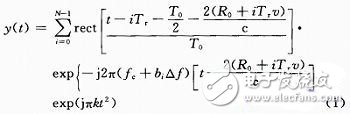
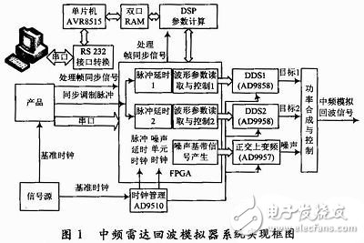
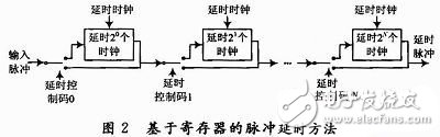
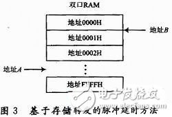
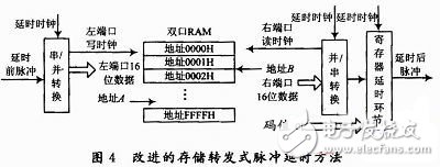
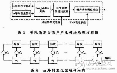
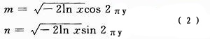
introduction In the development of various radar seekers, multiple tests are often required to verify the radar's analysis and processing performance of the target echo signals. However, although the field test is the most realistic simulation, it requires a lot of manpower and material resources, and the test cost is expensive. It is not suitable for performance evaluation in the development stage. It is usually only used as the final performance test after the completion of the missile development. Therefore, it is particularly important to be able to provide an electromagnetic environment that simulates real working conditions for radar seeker work in the laboratory. The radar echo simulator is developed to meet the above requirements. It not only saves designers a lot of development costs, but also shortens the development cycle and improves work efficiency. From the implementation method, the radar echo simulator is generally divided into two categories: storage playback and autonomous production. The storage playback type is based on the transmission signal modulation pulse of the frequency synthesizer receiving the radar product to be tested, and down-converts, samples and stores the transmission signal, completes the digital modulation processing of the target and the interference, and then passes the high-speed D/A and up-conversion. An implementation mode that is played back. The autonomous production mode does not need to receive the transmission signal of the product to be tested, but needs to obtain the clock and modulation pulse and the coherent frame synchronization signal which are in phase with the product. On this basis, a frequency complex similar to the product is adopted, directly according to the target and The interfering parameter information produces the analog echo signals required by the product. Both methods have their own advantages and disadvantages. The storage playback mode is insensitive to changes in the waveform parameters such as bandwidth, pulse width, etc., and can be automatically adapted; however, the frequency measurement processing under the condition of inter-pulse frequency agility is difficult to achieve quickly and accurately, and due to high-speed A/D Limitation, the signal-to-noise ratio of the analog echo signal is difficult to make high. The autonomous production circumvents the above-mentioned shortcomings of the storage playback type, but the changes in waveforms such as bandwidth and pulse width must rely on the product to provide information, and the flexibility is lacking. This paper discusses the design and implementation of an autonomous generation radar echo simulator IF part. The simulator can generate radar back of various waveforms such as pulse single frequency, pulse linear frequency modulation, step frequency, step frequency + linear frequency modulation. Wave signal, and can generate double-target and parameter-controllable band-limited Gaussian white noise, which can simulate the main interference type; the output signal can be directly used for the intermediate frequency injection test of the signal processor, or can be used for radar after up-conversion. Various test verifications under the system's RF conditions. The implementation method of the intermediate frequency radar echo simulator is described in detail below. 1 Theoretical analysis of echo signals According to the design requirements, the simulator needs to simulate pulse single frequency, pulse linear frequency modulation, step frequency, step frequency + linear frequency modulation of a total of four waveform signals. Among them, the step frequency includes two types: sequential step frequency and random step frequency. The radar echo signals of these waveforms can be uniformly expressed in the form of equation (1): Where: c is the speed of light; N is the total number of pulses of the coherent frame; i is the number of pulses in the coherent frame; To is the pulse width; Tr is the pulse period; fc is the first pulse in the coherent frame Frequency; Δf is the minimum step frequency difference between pulses; bi△f is the frequency change of the ith pulse on the basis of the initial carrier frequency (only applicable to inter-pulse frequency agile waveform, non-interpulse agile waveform is bi= 0);k is the rate of intra-pulse frequency modulation when the chirp waveform is (non-intra-linear chirping is k=0); Ro is the target current distance; v is the target current speed. From the above analysis, it can be known that regardless of the above-mentioned waveform, the delay of the pulse, the initial phase of the pulse of each pulse, and the carrier frequency of each pulse can be calculated according to the formula (1), and these parameters are in the product. On-the-fly control is based on real-time control. Depending on the transmitted waveform, it is also decided whether to add intrapulse frequency linear modulation. 2 echo simulator system design According to the system requirements and the aforementioned theoretical analysis of radar echo signals, the intermediate frequency radar echo simulator (hereinafter referred to as the simulator) adopts the system implementation scheme shown in FIG. The simulator performs asynchronous serial communication with the host computer through the single-chip microcomputer (AVR8515), and the single-chip computer completes the process of unpacking and packing the communication protocol, receives the target and interference parameters set by the user in the host computer, and transmits the real-time simulation state information of the simulator. Give the host computer. The system uses DSP (ADSP-21060) as the real-time calculation unit of pulse parameters. The MCU and DSP ask for information exchange through dual-port RAM. After the DSP obtains the simulation parameters of the two targets, according to the time tempo of the parameter change, the parameters such as the initial phase, the carrier frequency and the pulse delay of each pulse of the two targets of a coherent frame are calculated and written to the dual port RAM. The system uses FPGA (XC2V3000) as the signal processing and control unit. After the FPGA reads, it combines the waveform type information transmitted from the serial port of the product under the control of the frame synchronization signal and synchronous modulation pulse provided by the product (for example: intra-pulse single frequency). Or linear frequency modulation), forming a delay pulse of two targets, and controlling the respective DDS (AD9858) signal generating units of the two targets to generate two target signals. The digital quadrature baseband with limited Gaussian white noise is also generated by the FPGA and the digital quadrature upconversion function of the AD9957 is synchronized to modulate the baseband to the desired center frequency. The synthesis of target 1, target 2 and noise signals is realized by an analog circuit, and a certain power control is realized, and finally the required intermediate frequency radar echo signal is output. The phase-parameter of each unit clock of the simulator system is very important. The dedicated clock management chip (AD9510) generates the working clock of the FPGA, AD9858, and AD9957. 3 key module design 3.1 Digital Delay Module For the implementation of the digital delay of the pulse, the method 1 is to convert the delayed clock value D calculated by the DSP into a binary code of N bits, and control by using the binary code. It can be implemented as a register-based method as shown in Figure 2. The advantage of this method is that there is no fixed delay and zero delay can be achieved. However, when N is increased, the FPGA trigger resource consumed by this method increases geometrically, so it is not suitable for occasions where a large delay is required. The method 2 adopts the method of store-and-forward as shown in FIG. 3, specifically: the input delay pulse is sampled by the delay clock, and the left port address A is incremented by 1 during each delay clock cycle. In the single-bit dual-port RAM, the right port is incremented by 1 in each delay clock cycle with address B, and the left and right ports are automatically returned to the 0 address after the upper limit address of (2N+1-1). Incremental operation. Address A and address B satisfy: B=A-D. D is the value of the required delay clock. When A "D", take the complement of the negative number as the address B. Method 2 avoids excessive consumption of flip-flop resources under large delay conditions, but there is a fixed delay. When the delay clock frequency is high, the read/write speed of the dual-port RAM is difficult to meet the requirements. Therefore, the system has improved the design of Method 2 in practice, as shown in Figure 4. In this design, the pulse to be delayed is sampled by the delayed clock, serially converted to form 16 b of data, and each 16 delayed clocks are serially/parallel converted, and a 16 b wide dual port RAM is output left. The port writes the clock, and address A is still accumulated in order. Filling the last bit of address A with four "1"s constitutes a wide address x; x - D = Y (complement form); where: D is the value of the delayed clock calculated by the DSP. The lower four bits of Y (binary) are extracted as code value C; the remaining upper bits form the right port read address of the dual port RAM in the figure. The read clock is outputted by the parallel/serial conversion unit on the right side of each of the 16 delayed clock cycles, and the parallel/serial conversion unit converts the read 16-bit data into a pulse, which is implemented by the register mode as shown in FIG. After the delay of the register delay (control code is code value C), the pulse after the delay is output. The method reduces the read/write clock of the dual port to the frequency division of the delay clock by 16, which greatly reduces the speed pressure of the dual port RAM and is easier to implement. Another 16 b dual-port RAM can also be implemented with off-chip dual-port RAM, reducing the reliance on FPGA memory resources. The disadvantage of this method is that there is a larger fixed delay. Although the control value can be corrected by the DSP in advance when the delay is large, the case where the required delay is less than its fixed delay cannot be applied. The system is comprehensively solved by two methods, that is, the highest bit of the DSP output code value determines the switching of the delay method, and when the delay of the demand is greater than the fixed delay, the method of FIG. 4 is adopted; and the delay of the demand is less than the fixed delay. The register method of Figure 2 is used at all times. 3.2 Digital Noise Baseband Generation Module The noise baseband signal of this system is generated by digital technology and completed in FPGA. The implementation method is shown in Figure 5. According to the random signal theory, whitening processing of uniformly distributed random numbers can realize Gaussian white noise with good statistical characteristics. The system first uses two independent m-sequence generators to generate a pseudo-random number uniformly distributed in the interval [0,1]. The hardware structure of the m-sequence generator is shown in Figure 6, where Co and Cn are the coefficients of the corresponding m-sequence polynomial. , with values ​​0 and 1. Then, the generated pair of pseudo-random numbers can be obtained by Box_Muller transform to obtain a pair of mutually independent pseudo-random numbers m and n conforming to the standard normal distribution, which are just the in-phase component and the quadrature component of the noise generator. The Box_Muller transformation formula is: Where x: y is the aforementioned two pseudo-random numbers that are uniformly distributed on (0, 1). Since the Box_Muller transform requires two nonlinear functions, and the nonlinear operation is difficult to implement in the actual digital circuit system, it is necessary to construct a corresponding look-up table to realize the nonlinear operation, which is denoted as sqrt_lut and sincos_lut, respectively. Let the output quantized data lengths of sqrt_lut and sincos_Iut be L1 and L2 bits, and the fixed lengths of the independent variables m and n are N1 and N2 bits, respectively. Then, when using the uniform quantization scheme, the storage spaces required for sqrt_lut and sincos_lut are 2N1 & TImes; L1 and 2N2 & TImes; L2, respectively. It can be seen that if the lookup table function is directly implemented, when N1 and N2 are large, the corresponding storage space is considerable. To compress the storage space, for sincos_lut, only the sine and cosine values ​​of the first quadrant can be stored. The other quadrants are obtained by symbol adjustment, which can reduce the storage space occupied by sincos_lut to 1/4 of the original. Furthermore, it is also possible to perform a piecewise polyline approximation for the non-linear curve, and store only the starting position and corresponding slope of each polyline segment in the actual lookup table. It is also possible to drastically reduce the number of lookup tables required. This strategy also applies to the sqrt_lut lookup table. After obtaining a pair of mutually independent standard normal distribution variables m and n, they are also low-pass filtered to accommodate the corresponding signal bandwidth. Since the filtering characteristics of the I-channel and the Q-channel are exactly the same, in order to further save resources, a filter supporting two-channel operation can be used to simultaneously perform filtering of the I-channel and the Q-channel. This can be easily implemented through the FIR IP core in the Core Generator in the ISE integrated development environment. The filter system can transmit the corresponding coefficients to the DSP according to the required bandwidth by the host computer, and then pass to the FPGA. The noise power adjustment module can adjust the amplitude of the generated band-limited Gaussian white noise by multiplying the corresponding coefficient according to the set signal-to-noise ratio. 4 Conclusion Based on the principle of self-generation, this system selects DSP and FPGA as the core processor. Through reasonable algorithm design, the design of IF radar echo simulator compatible with multiple radar waveforms is realized, and the improved digital pulse based on store-and-forward is adopted. The delay method reduces the hardware requirements of the system while achieving a minimum delay step of 8 ns. Another key module of the system is the digital noise generator, whose parameters can be modified in real time, greatly improving the flexibility of the noise generator. Compared with other similar types of designs, it has fast working speed, high resource utilization, and hardware structure. Simple and so on. Finally, DDS, digital quadrature upconversion and other devices are used to achieve accurate complex frequency modulation, phase modulation and amplitude modulation, ensuring system flexibility, high compatibility and integration. Ultraviolet Bulb,T5 4 Pin Uvc Tube,T5 4 Pin Uvc Light,T5 4 Pin Uvc Bulb Changxing leboom lighting product CO.Ltd. , https://www.leboomuv.com