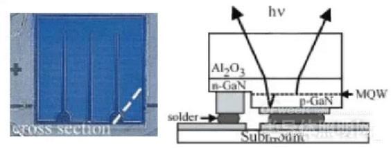
1 Introduction As a new type of green illumination source, LED ( LED ) has the advantages of energy saving, high efficiency, low carbon, small size, fast response, strong shock resistance, etc. It can provide users with a new lighting experience that is environmentally friendly, stable, efficient and safe. Developed into a mature semiconductor lighting industry. In recent years, countries around the world have begun to ban incandescent light bulbs, LED will usher in a golden period of growth. In addition, in recent years, LED applications in TV backlights, mobile phones, and tablet computers have also experienced explosive growth, and LEDs have broad application prospects. 2. Development and current status of flip-chip LED technology Flip-chip technology is still a relatively new technology concept in the field of LED, but it has been widely used and matured in the traditional IC industry, such as various ball grid array package (BGA), chip size package (CSP), wafer level chip. Technology such as size package (WLCSP) uses flip chip technology, which has the advantages of high production efficiency, low device cost and high reliability. The application of flip chip technology to LED devices is mainly different from IC. In the process of LED chip manufacturing and packaging, in addition to handling stable and reliable electrical connections, it also needs to deal with light problems, including how to make more light. Come out, improve the light extraction efficiency, and the distribution of light space. In 1998, JJ Wierer et al. prepared a high power of 1W flip-chip soldering structure for the difference in heat dissipation of conventional LEDs, uneven distribution of transparent electrode currents, surface electrode pads and lead light blocking, and reliability caused by gold wires. AlGaInN-LED blue chip, they flip-chip the metal bumped AIGalnN chip on a silicon carrier with an antistatic protection diode (ESD). Figure 1 is a photograph and a cross-sectional view of an LED chip prepared by them. Their test results show that, under the same chip area, the flip-chip LED chip (FCLED) has a larger light-emitting area and very good electrical characteristics than the packaged chip. In the current range of 200-1000 mA, the forward voltage (VF) Relatively low, resulting in higher power conversion efficiencies. Figure 1 Picture and cross-section of the LED chip of the flip-chip structure In 2006, OBShchekin et al. reported a new multi-quantum well structure LED (TFFC-LED) for flip-chip bonding. The so-called thin film flip-chip LED combines the concept of thin film LEDs with flip-chip LEDs. After the LED is flip-chip mounted on the substrate, the sapphire substrate is stripped off using a laser lift-off technique, and then the surface is roughened by photolithography on the exposed N-type GaN layer. As shown in FIG. 2, such a thin film structure LED can effectively increase light extraction efficiency. But relatively speaking, this structural process is more complicated and the cost will be relatively higher. Figure 2 Schematic diagram of the film flip chip LED chip structure Thermal Printers Cleaning Kits Cleaning Pen For Card Printer,Ipa Cleaning Pen For Card Printer,Pre-Saturated Ipa Cleaning Pen,Presaturated Ipa Wipes Miraclean Technology Co., Ltd. , https://www.mrccleanroom.com